Making PCB's on SL1S
With the higher UV output and monochrome screen of the SL1S, a thought hit me last week: Maybe it is possible to use it for exposing photosensitized printed circuit boards directly. Today I tested it, and it looks very promising.
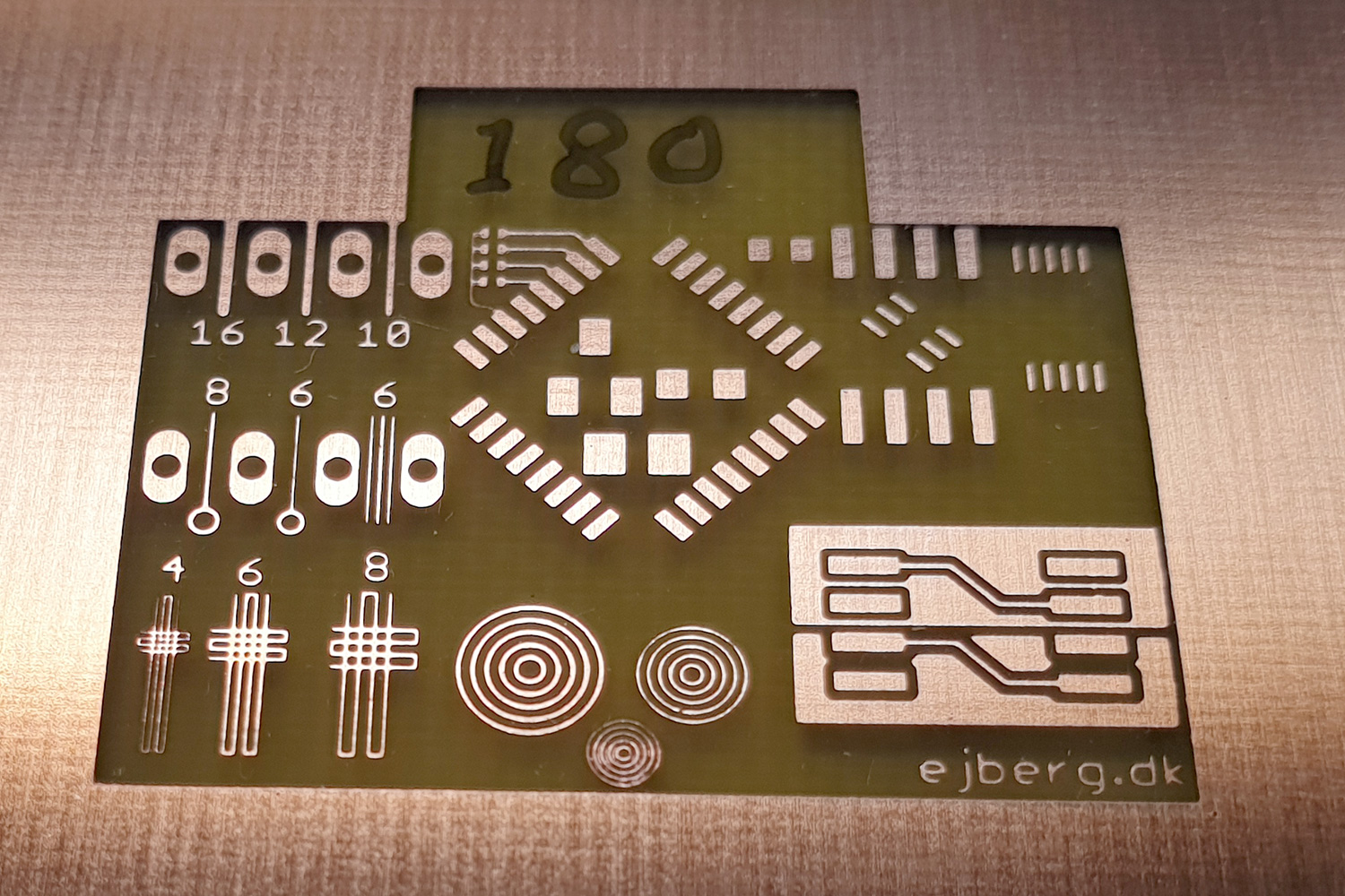
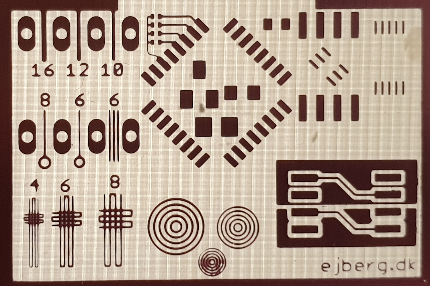
Here is my calibration test. The handwritten numbers are the exposure time in seconds. The built-in resin calibration function was used, but it can't write the exposure time when only "printing" one layer.
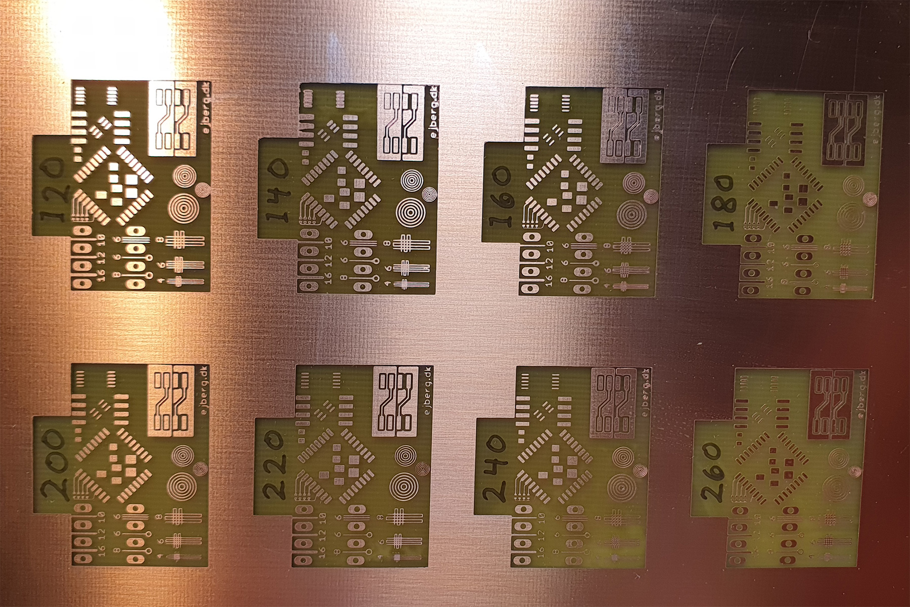
4 mil tracks (0.1 mm) are too small. 6 mil tracks looks possible if the pcb is exposed, developed and etched carefully. 8 mil tracks are no problem.
I need to experiment some more, but this looks promising.
RE: Making PCB's on SL1S
That is excellent! It makes perfect sense that it would work, but it hadn't occurred to me at all. You've just added another reason for me to "need" a MSLA printer and probably the SL1S. Nice!
RE: Making PCB's on SL1S
Would you mind if I posted a link of your results to the EEVblog forum about your results. This forum is about electronics. I am quite sure it would interest the folks in the 3D section of it.
Assuming someone does do it before I do.
Cheers.
REPAIR, RENEW, REUSE, RECYCLE, REBUILD, REDUCE, RECOVER, REPURPOSE, RESTORE
RE: Making PCB's on SL1S
Would you mind if I posted a link of your results to the EEVblog forum about your results.
Go ahead and do it. I don't mind at all.
I do have an account on EEVblog myself, but I haven't been active there for some time.
RE: Making PCB's on SL1S
Thanks. Done.
You can find the replies in their 3D printer section.
Hope you will keep posting your results as you push the limits of the technique.
Cheers.
REPAIR, RENEW, REUSE, RECYCLE, REBUILD, REDUCE, RECOVER, REPURPOSE, RESTORE
RE: Making PCB's on SL1S
Hope you will keep posting your results as you push the limits of the technique.
I will.
I am going to attempt to make some sort of alignment fixture, so it will be possible to make double sided boards.
RE: Making PCB's on SL1S
A little update. I am experimenting with a 3D printed (of course) fixture, that'll allow me to place a pcb into the old vat from SL1 (after upgrading to SL1S, the old vat was just collecting dust anyway). Using the vat allows for precise placement every time, as well as protecting the LCD from scratches.
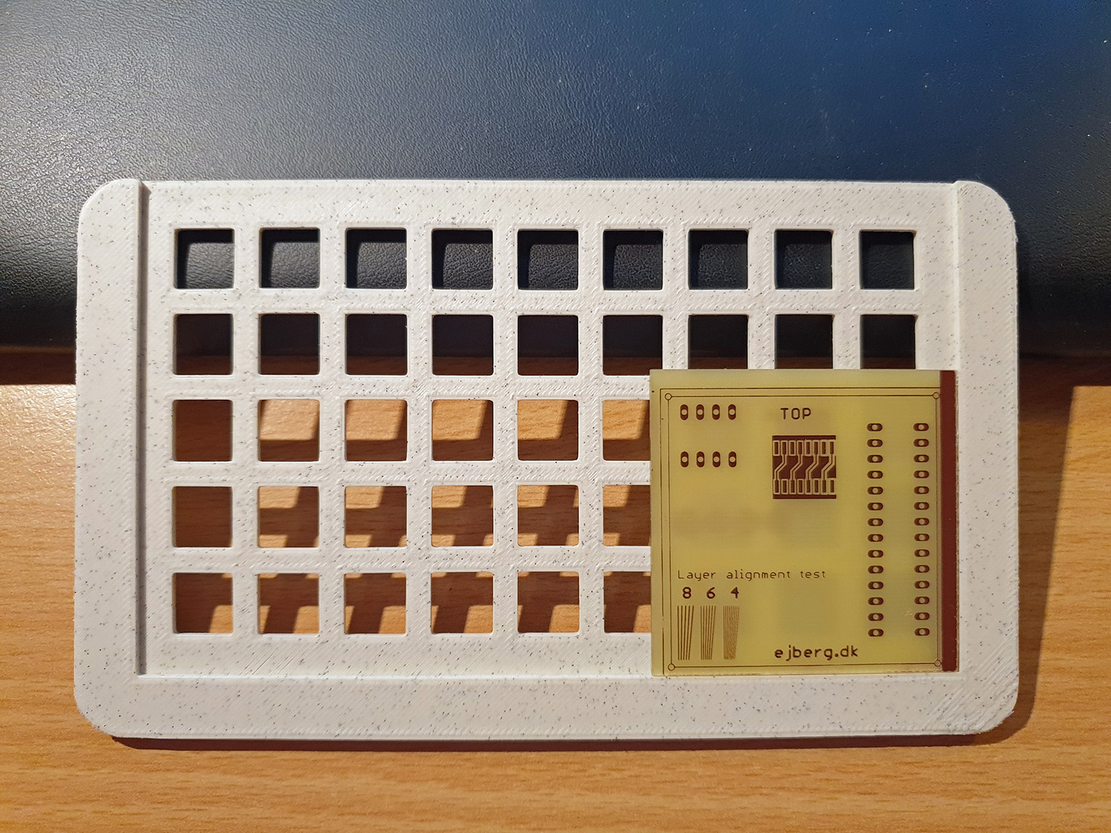

In this first attempt, the vertical alignment is perfect and the horizontal alignment is a little off (within 1 mm). Also, I seem to have reached the edge of the LCD (the thick line at the right). This should be easy to correct when preparing the image files for printing.
RE: Making PCB's on SL1S
Wow, so cool, how did you do that ?
How to get the Gerber / PDF / (Png?) Image on the SL ?
RE: Making PCB's on SL1S
Wow, so cool, how did you do that ?
How to get the Gerber / PDF / (Png?) Image on the SL ?
It takes some manual image manipulation.
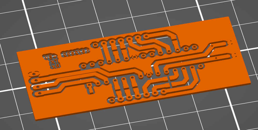
First, you must be able get the layout as some sort of image file. I use an old version of Eagle, and that can export to an image.
I haven't been able to find the exact data on the monochrome screen used in SL1S, but from indirect sources, I calculated the screen to be 1620 x 2560 with a resolution of 508 dpi. The resolution probably is a little off, but it's been good enough for my work. The trick is now to get the pcb layout into a grayscale .png with this resolution.
I export from Eagle in 4 times the resolution (2032 dpi), and in black/white only. I then use a photo editor to downscale to 508 dpi, while converting to a grayscale image. This provides anti-aliasing for slanted lines. Then I found a gamma correction of 0.7 improves the effectiveness of the anti-aliasing. Then the image is mirrored. Finally I copy/paste the layout into a 1620 x 2560 blank image and save it as .png
I then put the .png into a special .sl1s file I have prepared for pcb work. .sl1s files are just ordinary .zip files, so with a little renaming, it is possible to access its content. I have attached one of my test files, that can be used as a starting point. Just replace the .png inside the .zip, and yes, the filename matters. Keep the name as it is, or edit config.ini if you want to change it.
Then just rename the .zip to be .sl1s. Put it on an USB stick, put a photosensitized pcb in the printer and "print" a pcb. Make damn sure you DON'T have the build platform mounted in the SL1S, or it will come down and press on the pcb (and the LCD). Also, disable the resin level check or the print will fail.
RE: Making PCB's on SL1S
Instead of editing Images, I could export the PCB als STL (using Fusion 360).
Now I would like to slice it with all checks and movement disabled (or remove it from the gcode), so I can lay it (extremely careful so not to scratch it) direct on the screen of the SL1. Using only the screen and the UV light, nothing else.
Can that be done ?